
Sil-More Newsletter - Issue 19 - Friendly Environment New Materials: Solvent-Free Three-Proof Adhesive
2018/09/22|Subscribe to the newsletter
Friendly environment new materials solvent-free three-proof adhesive
 Friendly environment new materials solvent-free three-proof adhesive

In industrial processes, chemicals often contain benzene or solvents, which are volatile and mostly harmful to human health. In recent years, European and American countries have been regulating the content of such chemicals. Even China, as the world's largest manufacturing region, has gradually begun to pay attention to environmental protection and pollution measures in recent years, which has become a policy trend. After the "19th National Congress", the draft constitutional amendment in mainland China included "building a prosperous, democratic, civilized, harmonious, and beautiful socialist modernized strong country", which means that future topics related to environmental protection and "Beautiful China" have been incorporated into the constitution. It can be expected that the world's emphasis on environmental protection awareness will likely lead to many measures for pollution prevention and protection of human health being introduced.
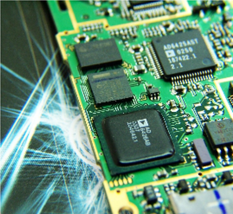
In the electronics industry, it is common to use coating materials. A layer of adhesive is evenly coated on the surface of PCB and PWB boards or in specific areas, mainly used to protect reliability, achieving moisture-proof, insulation, and dust-proof effects. This addresses issues such as electronic products absorbing a large amount (or trace) of moisture over a short (or long) period, leading to losses, reduced efficiency, R&D failures, high defect rates, and poor reliability, ensuring that circuit board assemblies can operate more stably under required environmental conditions and over a longer lifespan.
The EU has regulatory requirements for toluene in solvents:

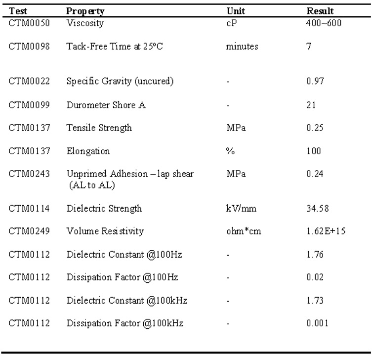
In recent years, environmental protection trends have changed processing habits. The materials used in product processes must contain low levels of benzene, formaldehyde, acetone, and xylene to meet EU environmental standards. Therefore, major manufacturers around the world have gradually strengthened regulations on solvent-containing chemicals. For example, many years ago, Foxconn Technology Group completely banned the purchase of chemicals such as benzene or n-hexane. As a result, the internationally renowned chemical materials giant Dow DuPont launched a new brand - DOWSIL™ EA 9187 LH, a new solvent-free three-proof adhesive, which can be used for PCBs and PWBs in all products requiring waterproof, dustproof, and anti-static properties, whether for various outdoor electronic products, LED lighting, automotive electronics, power supplies, network communication devices, control modules for machine tools, or various indoor electronic devices and mobile devices, achieving good protective effects (product information as follows).
Product features:
|
Product specifications:
Facing the rapidly changing trends in the manufacturing industry, Sil-More Industries has long been deeply involved in the high-tech industry, leading the way in sharing various new material options corresponding to the future development of the electronics industry, providing the most complete adhesive supply and professional consulting services.
※ Reference website:https://www.researchmfg.com/2011/09/conformal-coating/
── Written by: Business Department David Chen
Full lamination process application for touch panels

With the rapid popularization of smart products, from portable handheld devices to large displays, outdoor billboards, and even in-vehicle displays and curved panels, users continuously pursue thinner, smaller, and better display effects, prompting major manufacturers to strive for breakthroughs in lamination technology to provide optimized screen presentation effects. Currently, the existing full lamination technology can significantly reduce light reflection, minimize light loss, enhance original brightness, and improve overall display effects; at the same time, the bonding strength of full lamination is higher than that of traditional edge bonding, reducing interference with touch signals and enhancing the smoothness of touch functionality.
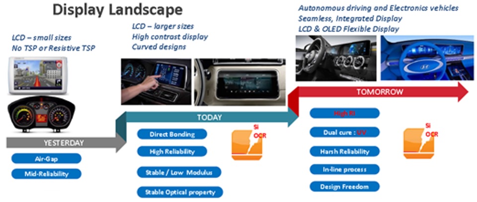
In full lamination materials, there are two processes: solid transparent optical adhesive (OCA) and liquid transparent optical adhesive (LOCA/OCR). The former is a roll film material, while the latter is a liquid optical adhesive. OCA is widely used because of its fast processing speed, and early requirements for yellowing were not so strict. Acrylic-based OCA is inexpensive and has strong adhesion, making it the best choice for consumer products. OCR is divided into acrylic-based and silicone-based, with the former mostly using UV rapid curing, also applied to non-outdoor products with less stringent weather resistance requirements, while the latter is used for products that are strict on temperature and humidity testing, such as military tablets, automotive panels, and outdoor displays. Early silicone-based OCRs were all heat-cured or room temperature cured.
In the past two years, the demand for outdoor displays, automotive, and military control products has increased, and the testing specifications for the materials used have become increasingly stringent, especially for yellowing resistance and high temperature and humidity thresholds. Therefore, the weather resistance characteristics of silicone-based materials have become more favored. To balance product weather resistance and pursue production capacity, major manufacturers have launched UV curing and rapid curing silicone-based OCRs. Through UV curing, the full lamination of touch panels and glass protective layers can be completely cured in just a few seconds, even without equipment; using rapid curing only requires twenty minutes of room temperature standing to achieve complete curing, providing the best lamination solution for display products.
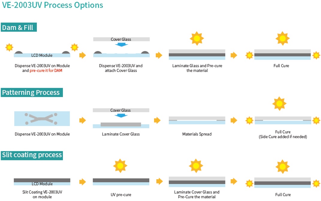
Sil-More provides full bonding materials, representing the internationally renowned chemical materials manufacturer Dow DuPont's new brand - DOWSIL™ OCR VE-2003 UV optical curing silicone. It has also gained recognition from well-known brand manufacturers and first-tier OEMs in South Korea, Taiwan, and Japan. The original manufacturer is actively continuing to improve product characteristics to better meet customer requirements. In terms of product layout, plans are underway to gradually launch various bonding applications with different characteristics such as fast curing (Snap cure) and dual-component UV curing, to meet the high display quality and yield requirements that many customers pursue in optical full bonding processes.
─Written by: Business Department Ashley Chiu
New generation semiconductor packaging technology evolution

The semiconductor industry is a major lifeline supporting Taiwan's economy, with the IC industry's output value ranking third globally, making it one of the leading countries in guiding industry development. Taiwan's wafer foundry and IC packaging and testing industries rank first in the world. According to data released by the World Semiconductor Trade Statistics (WSTS), the global semiconductor market is expected to reach $463 billion in 2018, a 12.4% increase from 2017. WSTS estimates that the global semiconductor market will grow to $463 billion and $484 billion in 2018 and 2019, respectively. As the industry model shifts, Taiwan's IC industry continues to provide professional wafer manufacturing services to the international market, investing in R&D and expanding production capacity, deeply cultivating the global IC packaging and testing market, and accelerating the development of advanced packaging technology, creating an indispensable energy for the international IC industry.
With the continuous integration and innovation of electronic communication products, the portable electronic product market is booming. The demand for semiconductor IC (Integrated Circuits) packaging technology requires not only compactness but also high-speed and multifunctional chip module systems. For new product design trends in mobile network transmission, wearable product applications, the Internet of Things, and automotive communication, chip packaging sizes are becoming smaller, and the number of required pins is increasing, leading to higher reliability requirements for packaging processes. Traditional semiconductor packaging technology can no longer meet the current demands for high density, multifunctional heterogeneous integration, high transmission efficiency, and low cost in chip packaging products. For example, chip size packaging technology (CSP) is evolving towards wafer-level chip size packaging (WLCSP) technology to improve production efficiency and reduce costs.
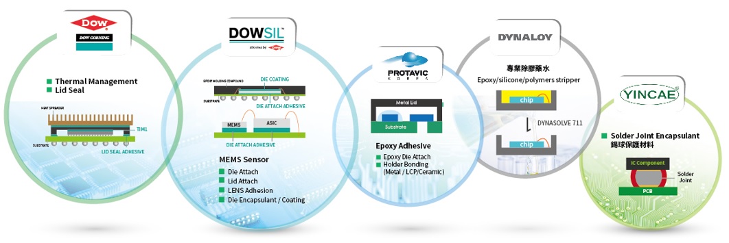
In the packaging process, flip chip packaging structures have become mainstream in the market, with increasing material property requirements. Most packaging material manufacturers face low-margin growth situations and need to seek low-cost packaging solutions. From a material technology perspective, Sil-More Group represents and sells internationally renowned leading brand adhesives, successfully promoting various packaging process application adhesives to Taiwan's semiconductor packaging field to meet the requirements for high adhesion, excellent electrical insulation, high thermal conductivity, low moisture absorption, and low molding shrinkage. For example, providing high thermal conductivity conductive silver adhesive (TC>20W, PROTAVIC Sintering silver ACH35006) for die attach in advanced packaging processes; launching solder joint encapsulant (YINCAE SMT256/BP256) that can replace underfill in BGA and SMT; new technology nano-level underfill adhesive PRE-UNDER FILL (YINCAE SMT158); high adhesion strength lid attach/glass bonding materials (thermosetting/UV curing/B-Stage, PROTAVIC S-J(M-1)HV) for SENSOR packaging; thermal management applications and heat spreader lid seal for FLIP CHIP BGA, Dow Corning™ SE4450, TC 3040, EA6900; and providing diversified material choices for MEMS and InFO packaging.
In recent years at international electronics exhibitions, it can be observed that products related to voice control and voice assistants, as well as 5G, the Internet of Things, AI, automotive networking, and self-driving cars are closely related to semiconductor development. In the future, the growth rate of industrial and automotive semiconductors will be the highest, and the combination of AI and IoT applications will lead to significant growth in the proportion of semiconductors in data processing applications. Therefore, to meet the increasing demand for heterogeneous integration of chips in end products like the Internet of Things, semiconductors have become a key driving factor. Sil-More Group actively connects the semiconductor-related industry chain under the current trends in semiconductor packaging technology development and the future industry's high specifications for new materials, focusing on the diverse application characteristics of semiconductor optoelectronic packaging materials, collaborating with original manufacturers to develop new adhesive applications, providing customers with highly reliable packaging materials and the best complete one-stop cross-domain material integration, and advancing towards the development of advanced packaging adhesives to enhance international competitiveness and seize more future business opportunities with customers.
Reference source:
IEKIndustry Intelligence Network(2018SemiconductorIndustry Yearbook
Ministry of Economic Affairs Investment Business Office (Taiwan Key Development Industry - Semiconductor)
DIGITIMEShttp://bit.ly/2MtOI3q ; http://bit.ly/2MvXIoC
Financial Newshttp://bit.ly/2MsNdm5
GO TOP─Written by: Business Department Russia Su
SPC statistical process control - CPK

SPC (Statistical Process Control) is one of the essential quality management techniques, applicable not only to manufacturing but also to non-manufacturing industries, e.g., hospitals, financial institutions, hotels.
Cpk (Process Capability Index) is one of the tools used in SPC, collecting control data from long-term, multi-batch production.
It uses some simple numerical values to assess whether a process meets product specification capabilities.
Cpk value is a composite indicator of Cp (precision) and Ck (accuracy). Currently, big data can be applied to software calculations to obtain Cpk, Cp, and Ck values, so it is necessary to interpret the significance of each numerical indicator and implement corresponding quality management measures.
1. Ck process accuracy: Indicates the percentage deviation of the measured value from the specification center value. The smaller the deviation from the center value, the more accurate it is, so a smaller Ck value is better.
2. Cp process precision: Indicates the ratio of the specification tolerance range to process variation (6σ). The smaller the process variation, the better the process precision, so a larger Cp value is better.
3. Cpk process capability index: Indicates the process capability index after integrating Ck and Cp. Process capability needs to be accurate and stable, so a smaller Ck (accurate) and a larger Cp (stable) result in a larger Cpk value, indicating better process capability, with the same judgment as Cp.
Data reference: China Productivity Center - 8D Method - Enhancing Problem Analysis and Solving Ability Course Materials.
─Written by: Technical Department Hughes Chu
2018 Q3 Exhibition Highlights
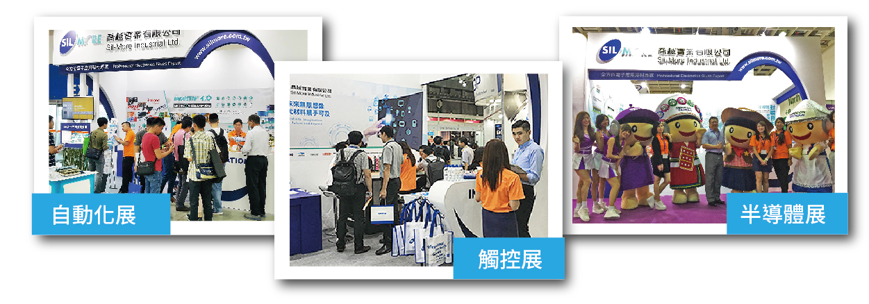
The convenience of smart IoT technology has created new economic development, with emerging industries rapidly emerging. This quarter's exhibition focuses on intelligent automation, touch panels, and semiconductors, showcasing a full range of key material solutions such as optical full lamination processes, IC component packaging, LED module packaging, and equipment maintenance lubrication at various exhibitions. We also provide vertical integration across industries, offering a complete display and explanation of the corresponding materials from upstream, midstream, downstream processes to end products, attracting many potential customers for consultation on-site, and providing professional services and high-quality products for better demand matching, jointly creating future business opportunities!
Exhibition Information Inquiry:
8/1-8/4 Taipei International Automation Industry Exhibition https://www.autotaiwan.com.tw/
8/29-8/31 Smart Display and Touch Exhibition https://www.touchtaiwan.com/
9/5-9/7 International Semiconductor Exhibition http://www.semicontaiwan.org/en/
─Written by: Marketing DepartmentGO TOP
Taipei headquarters annual employee trip
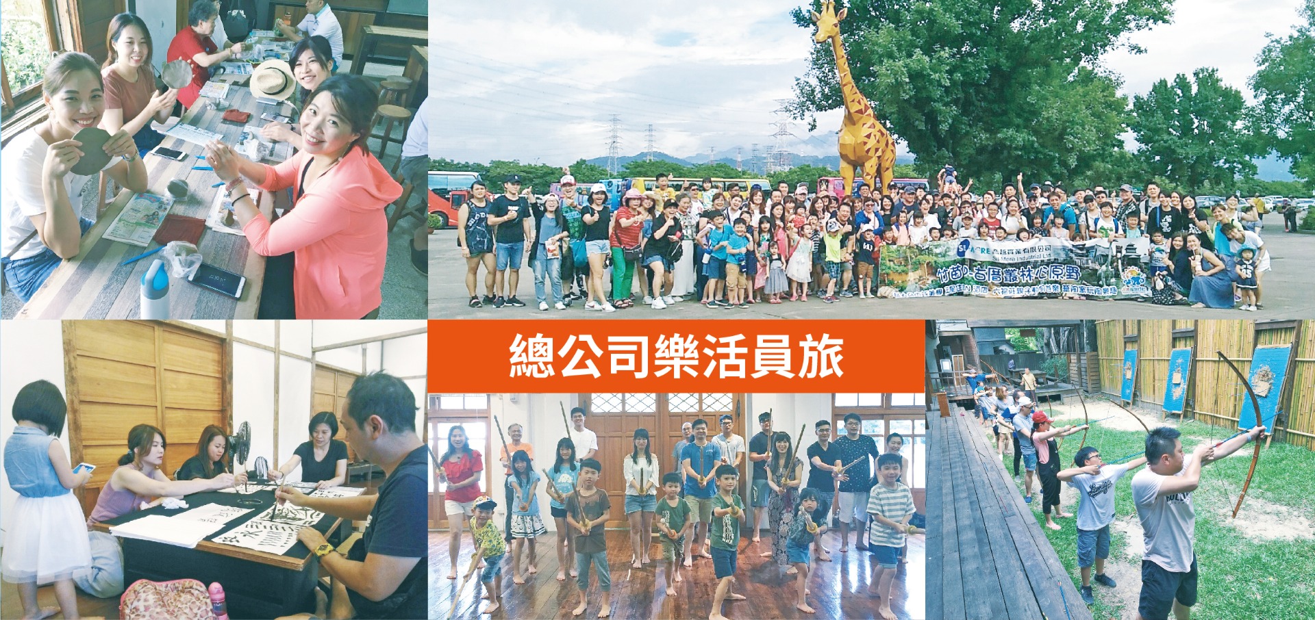
Summer vacation is here~ To reward employees, we are holding a special employee trip, allowing colleagues more time to gather with their families, while continuously improving work efficiency and effectiveness. Sil-More Industrial Co., Ltd. holds an employee trip every year, and this year is no exception. The three-day, two-night trip to New Zhong Liufu Village will happily commence from July 19 to July 21.
Boarding the exclusive Sil-More Industrial tour bus, we enjoyed the beautiful scenery and arrived at Miaoli Huatao Kiln, a place rich in cultural significance. Colleagues and their families could enjoy DIY pottery together, and through the guided tour, we gained a deeper understanding of the intricacies of garden landscape architecture. We experienced rural charm and tasted delicious rice meals; in the afternoon, we arrived at the Audit New Village, an emerging cultural and creative settlement. Converted from old dormitories, many shops have settled in, gathering many nice stalls~ it has a strong artistic atmosphere, while another group of colleagues went to the Qinyi Green Park shopping mall~ which is also quite enjoyable. In the evening, we checked into the newly opened Taichung Lin Hotel in 2015. After a hearty meal, the night was free for activities, and colleagues could visit the nearby Fengjia Night Market or enjoy the hotel facilities, ending this fulfilling day.
On the second morning, some colleagues chose to wake up early to stroll in Qiu Hong Valley and enjoy the greenery of the ecological park. At noon, we went to the super hard-to-book Taichung BBQ restaurant, Yi Ge Wu Ma BBQ, and enjoyed a very filling meal to replenish our energy. In the afternoon, we arrived at the Daohe Six Arts Cultural Center, the only remaining martial arts dojo-style Japanese building in Taichung City, which has nearly a hundred years of history. Here, we offered kendo, archery, tea ceremony, and calligraphy for colleagues to choose from, allowing them to settle their minds through these traditional skills. That evening, we stayed at the Liu Fu Village surrounded by animals, enjoying the healing feeling brought by the lovely animals.
The next day was spent enjoying Liu Fu Village. In addition to the original land-based amusement facilities, the latest water park was also opened, allowing all adults and children to happily and satisfactorily conclude this three-day employee trip.
─Written by: Marketing Department
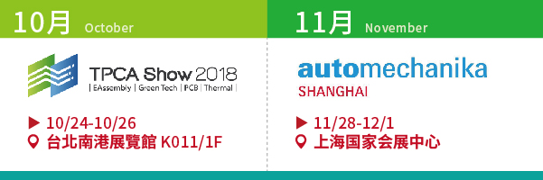
2018 Q4 exhibition preview
─Written by: Marketing Department Marketing

China Kunshan Subsidiary
TEL:+86-512-5778-9977
FAX:+86-512-5778-9944
E-Mail:silmore@silmore.com.cn
Website:http://www.silmore.cn/
Address: 13th Floor, Building 4, Chengbei Lake Commercial Center, 1188 Chengbei Road, Yushan Town, Kunshan City, Jiangsu Province, 215300
China Dongguan Subsidiary
TEL:+86-769-8541-8158
FAX:+86-769-8541-9158
E-Mail:service@silmore.com.cn
Website:http://www.silmore.cn/
Address: No.8 Huafu Road, Shangsha No.6 Industrial Zone, Chang 'an Town, Dongguan City, Guangdong Province, China 523000