

Sil-More Newsletter - Issue 8: The Most Promising CSP LED Packaging Technology
2015/11/05|Subscribe to the newsletter
HOT! The most promising CSP LED packaging technology
Green enterprises create the future with you
Fourth quarter exhibition information - Welcome to visit and guide
 HOT! CSP LED the most promising packaging technology
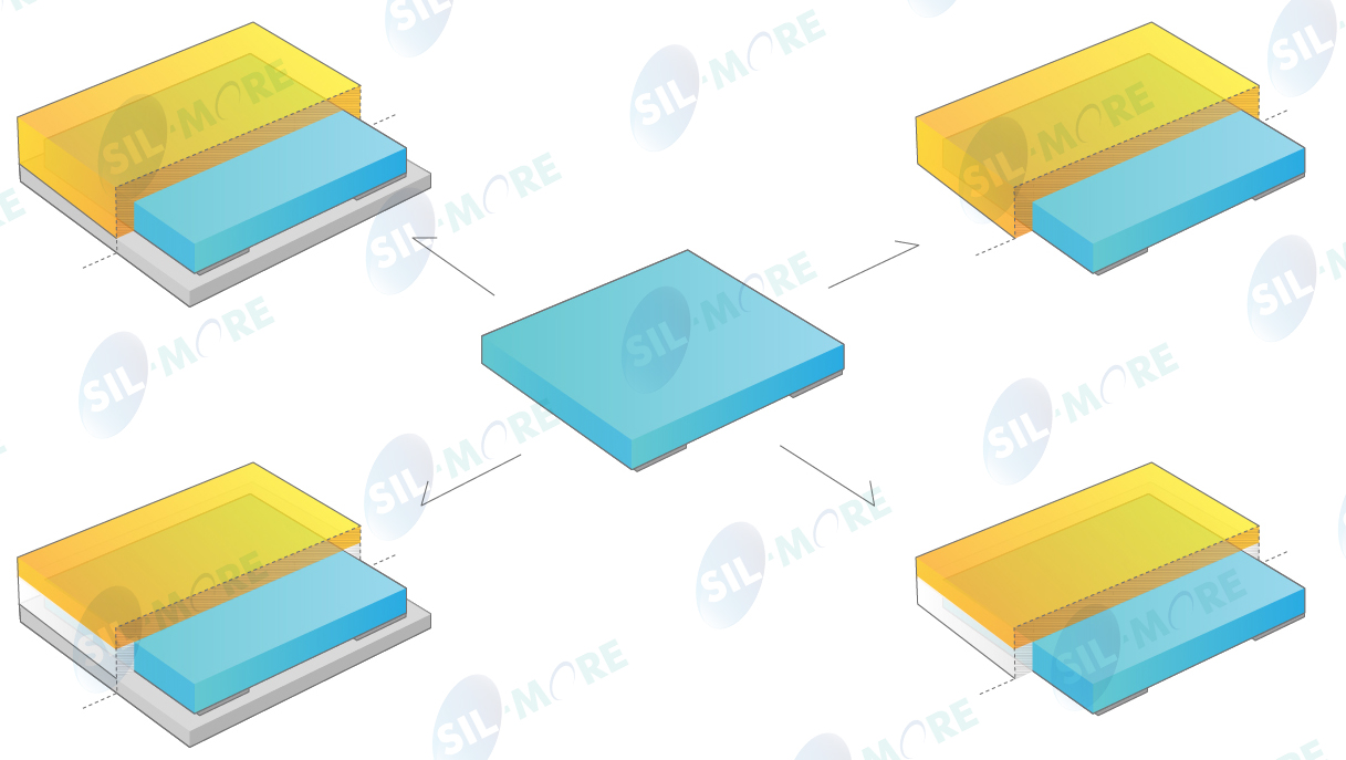
What’s CSP Chip Scale Package, abbreviated as CSP, which means chip-level packaging. CSP has the following advantages: the packaging body is miniaturized, suitable for various small, light, and thin products. It can be used as KGD (Known Good Die) in MCM applications. It has packaging (PGK) functions, which include: a. chip protection function b. stress relief function c. size matching (spacing transformation) d. standardization of specifications e. safe and convenient operation f. can utilize existing industrial infrastructure from shipping, testing, sorting to PWB assembly, almost all can use existing industrial equipment.
Chip Scale Package LED, abbreviated as CSP LED, means wafer-level packaged LED. It achieves vertical stacking packaging directly on the epitaxial chip, that is, directly packaging the entire chip and then cutting it into single LED (IC) chips. After 2010, the flip-chip LED, inverted LED, Flip Chip LED, FC LED, and non-packaged LED used in the LED industry refer to this wafer-level packaged LED (Chip Scale Package LED) as the correct name. The CSP LED packaging method has the shortest signal wire and energy conduction path, with the following advantages: 1. It not only has chip size packaging (CSP). 2. Thin packaging. 3. Packaging costs are lower than traditional methods. 4. High reliability. 5. Good heat dissipation (short thermal conduction path). 6. Excellent electrical properties (short wiring in packaging results in low inductance and capacitance). 7. Can use existing SMT equipment. 8. Quick assembly on the board and other advantages.
New! Application of adhesive film cutting materials
The adhesive film is used for various temporary adhesive fixing processes, which can be removed by heating or UV light after the processing is completed or semi-finished products are made.Electronic and optoelectronic industry component manufacturing and processing engineering, for example: LCD or touch panel glass grinding and polishing, LED cutting grinding polishing, cutting grinding polishing, EMC cutting, temporary fixing of semiconductor packaging cutting to facilitate grinding, cutting, fixing, and protecting circuits or board surfaces to avoid scratching the touch panel processing glass and adhesion between them.
The characteristics are similar to ordinary tape at room temperature, can adhere to objects, has excellent initial adhesion, good contact and cohesive solvent resistance, and can be easily peeled off with simple heating or UV light without causing any damage to the adhered object.
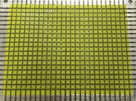 | 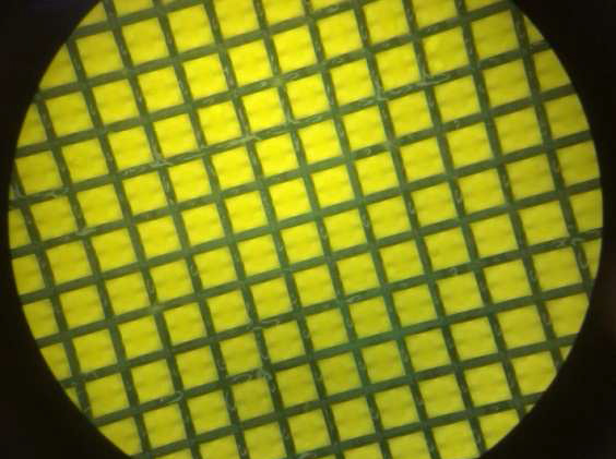 |
Before adhesive film cutting | After adhesive film cutting |
ReliableIGBTModule packaging solutions
AOS-IGBT applicationsIn recent years, due to the increasing emphasis on green energy, the demand for technologies such as smart grids, electric vehicles, wind and solar power generation has grown, and the demand for energy saving in households and industries has also increased, making power electronics technology increasingly important. With the development of power electronics technology, energy conversion efficiency continues to improve, especially the development of Insulated Gate Bipolar Transistor (IGBT), which performs excellently in energy-saving characteristics, further advancing the power electronics industry into another stage.
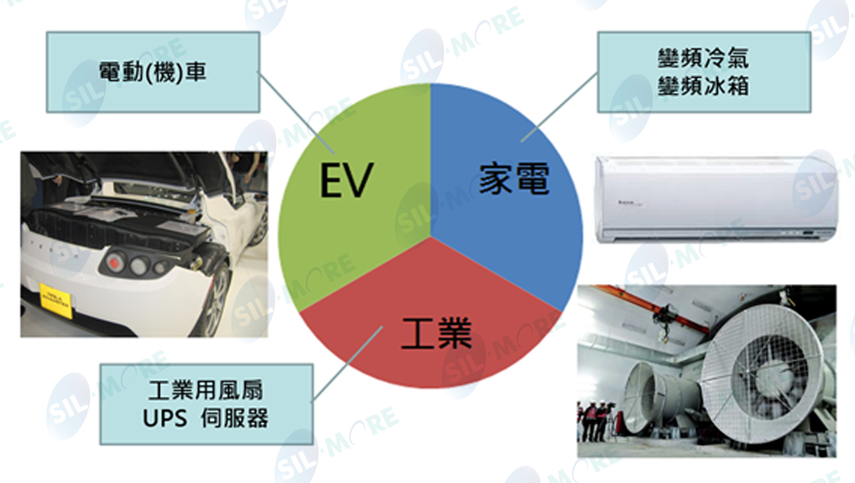
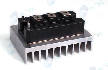
Due to the harsh application environment of IGBT power modules, the reliability of module packaging is relatively important, and one of the main reasons affecting reliability comes from heat issues. The heat generation per unit area and stress value of IGBT power modules have significantly increased, leading to thermal energy accumulation affecting product reliability, which has become a technical bottleneck.
The general method of heat dissipation will conduct the heat generated by the chip operation of the IGBT power module through thermal interface materials to the heat sink. Thermal grease is a commonly used interface material for IGBT power modules, mainly used to fill the micro-gaps and uneven surfaces generated when two materials contact, reducing interface thermal resistance and improving the heat dissipation performance of the device.
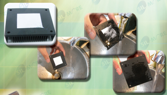
Sil-More further provides AOS non-silicone thermal grease for customers to choose from. Non-silicone thermal grease does not contain the silicone oil commonly found in general thermal grease, is not prone to separation or oiling before use, and is less likely to crack after use within the temperature range, and has the feature of being washable with water. The washable feature eliminates the need to use solvents that may pose fire hazards or environmental risks for cleaning. Therefore, AOS non-silicone thermal grease has become the specified thermal interface material for many customers on IGBT power modules.
The reliability requirements for the packaging technology of IGBT power modules are very high. In addition to being high specification and lightweight, the thermal design technology is crucial, and how to reduce thermal resistance through integrated system design is even more important for the overall product lifespan in the future.
Laboratory case sharing
Quality assurance laboratory case sharing§ Pot Life & Cure TimeMeasurement- 2015Year2MonthPot life, also known as Working Life or Usable Life, generally refers to the time when the resin viscosity is less than 10,000 cps, or the time when the viscosity becomes twice the initial value, and the definition varies with the type of resin and application method. Cure Time refers to the time it takes for the resin to dry and harden from a viscous state due to heat.
Pot Life and Cure Time can be measured using a viscometer. Taking epoxy resin EF 473 A(LH)/ BLR as an example, the viscosity is measured at 25 ℃ and 60 ℃, recording every 5 or 10 minutes to observe viscosity changes (Figures 1 and 2). To avoid damage to the instrument due to resin curing, each test should not exceed 800,000 cP. The viscosity reaching 10,000 cP is defined as Pot Life, and exceeding 1,000,000 cP is defined as Cure Time. From the two figures below, the Pot Life at 25 ℃ and 60 ℃ is 200 minutes and 40 minutes respectively. If the curve is extended, it can be inferred that the Cure Time at 25 ℃ and 60 ℃ is approximately 76 minutes and 590 minutes respectively. Because high temperatures accelerate chemical reactions, both Pot Life and Cure Time at 60 ℃ are significantly shorter than at 25 ℃.
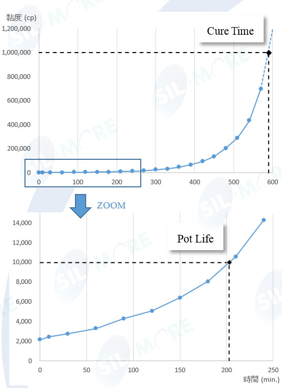
The Pot Life and Cure Time of materials are important information during use, and the measurement method is simple. By using a viscometer along with a constant temperature device, the Pot Life and Cure Time at different temperatures can be accurately measured. This meets more requirements in the process when providing products to customers.
─Written by: Technical Department Edmund Wu
Green enterprises create the future with you
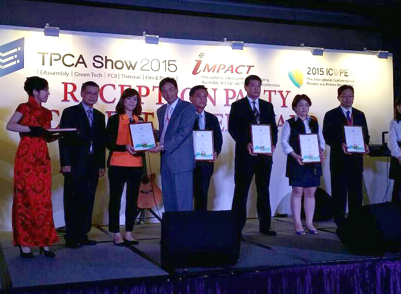 Support green exhibitions, love the environment and the earth, and contribute to society.
Congratulations to Sil-More Industries for winning the Excellence Award in the IECO Design Competition for Green Decoration at TPCA SHOW 2015.
─Written by: Marketing DepartmentGO TOP
Fourth Quarter Exhibition Information-You are welcome to visit and provide guidance.
|
|
|
Shanghai New International Expo Center W1-1A091 | China Shenzhen Convention and Exhibition Center Hall 2 2J65 | China Shenzhen Convention and Exhibition Center Hall 1 G138 |



China Kunshan Subsidiary
TEL:+86-512-5778-9977
FAX:+86-512-5778-9944
E-Mail:silmore@silmore.com.cn
Website:http://www.silmore.cn/
Address: 13th Floor, Building 4, Chengbei Lake Commercial Center, 1188 Chengbei Road, Yushan Town, Kunshan City, Jiangsu Province, 215300
China Dongguan Subsidiary
TEL:+86-769-8541-8158
FAX:+86-769-8541-9158
E-Mail:service@silmore.com.cn
Website:http://www.silmore.cn/
Address: No.8 Huafu Road, Shangsha No.6 Industrial Zone, Chang 'an Town, Dongguan City, Guangdong Province, China 523000